Five facts you must know about Intel glass substrates

【Lansheng Technology News】Intel provided more details about glass substrates at its annual event and promised to provide 1 trillion transistors in packages by 2030. At the Intel Innovation event in San Jose, California, the company also announced that mass production of glass substrates will begin between 2026 and 2030.
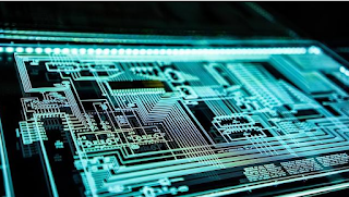
Intel has demonstrated a fully functional test chip using a 75um through-glass via with a 20:1 aspect ratio and a 1mm core thickness (Figure 1). So what is a glass substrate? How is it different from traditional epoxy ceramic and organic substrates? To understand this new chip substrate design, you need to know these five basic facts.
1. A brand new technology
Intel began producing glass substrates at its factory in Chandler, Arizona, nearly a decade ago. The semiconductor giant has reportedly invested more than $1 billion to achieve this goal, while building a new production line for this organic substrate alternative. The glass substrate R&D line has 600 employees.
This new glass substrate for chip packaging enables tighter signal spacing compared to organic substrates. It promises to bring speed and power benefits to large, power-hungry chips in servers and data centers. When the industry shifts to chiplet technology, which integrates multiple chips into one package, glass substrates will also come into play.
2.Technical advantages
Glass, whose main component is silica, is more stable at high temperatures. As a result, glass substrates can handle high temperatures more effectively while effectively managing heat dissipation for high-performance chips. This brings excellent thermal and mechanical stability to the chip.
Second, glass substrates enable higher interconnect density, which is critical for power transmission and signal routing in next-generation packaging. It is expected to greatly improve the connectivity of transistors within chip packages. A typical use case, chip packaging requires very dense interconnections between chiplets to ensure that the package does not bend during production.
Additionally, glass becomes flat more easily, which makes packaging and photolithography easier. According to sources, the glass substrate can reduce pattern distortion by 50%, thereby increasing the focus depth of photolithography, thereby ensuring more precise and accurate semiconductor manufacturing.
3. Why is the time to launch now?
Glass substrates not only overcome challenges such as interconnect density and temperature tolerance. Glass substrates also excel in mechanical and electrical properties and are not as undesirable as organic substrates when making very large chips. These substrates can accommodate 10 times the number of power and data connections than today's organic substrates. This is critical for large chips serving data artificial intelligence (AI) and high-performance computing (HPC) applications.
Intel believes that ceramic and organic substrates will reach the limits of their capabilities in the next few years. Intel says that by the end of the century, the semiconductor industry will reach its limits on the ability to use organic materials to scale transistors on silicon packages. Therefore, at a time when scale is critical to the progress and development of the semiconductor industry, glass substrates are a viable and essential next step for next-generation semiconductors.
4. Intertwined with packaging and small chips
The concept of glass substrates is closely related to advanced packaging and chiplet initiatives. The substrate is the medium where the chip die is located and plays an important role in chip packaging. While ensuring the structural stability of the chip, the substrate also carries signals from the chip die to the package. Therefore, their superior mechanical stability and higher interconnect density will help create high-performance chip packages.
First, glass substrates enable higher interconnect densities, allowing more transistors to be connected in a package. It is worth noting that Intel introduced glass substrates while building multi-chip system-in-package (SiP) mainly for data centers.
In fact, glass substrates are more suitable for small chips that integrate more transistors in a single package. Due to increased interconnect density, the substrate is able to accommodate more connections between chiplets, which also results in more chiplets being accommodated in the package.
5. Are there any difficulties?
If glass substrates embody this game-changing leap, what's the difficulty? "Basically, the innovation is complete," said Ann Kelleher, Intel's executive vice president of technology development. This sounds like a subtle hint at cost; glass substrates will be more expensive to produce and package than tried-and-true organic substrates. So, there may be yield issues initially.
More importantly, glass substrates need to establish a viable commercial production ecosystem. This includes necessary tools and supply capabilities. That's why Intel works closely with glass processing equipment and materials suppliers. The company also must find ways to outsource the testing and assembly of these new substrates.
The Santa Clara, California-based chipmaker plans to make glass substrates available to its Intel Foundry Services (IFS) customers in due course and is confident it will eventually bring the cost of glass substrates down to levels comparable to organic substrates. At the same time, Intel acknowledged that glass and organic substrates will coexist in the coming years.
Although Intel likely won't have exclusive access to glass substrate technology, glass packaging could still give Intel a huge competitive leap, especially for high-end chips serving artificial intelligence and data centers. After all, this will be a major technological transformation.
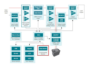
Lansheng Technology Limited, which is a spot stock distributor of many well-known brands, we have price advantage of the first-hand spot channel, and have technical supports.
Our main brands: STMicroelectronics, Toshiba, Microchip, Vishay, Marvell, ON Semiconductor, AOS, DIODES, Murata, Samsung, Hyundai/Hynix, Xilinx, Micron, Infinone, Texas Instruments, ADI, Maxim Integrated, NXP, etc
To learn more about our products, services, and capabilities, please visit our website at http://www.lanshengic.com
Comments
Post a Comment